In the realm of industrial automation and control systems, the demand for tailored sensing solutions is paramount. Custom proximity sensor schematic design represents a critical engineering discipline, bridging the gap between standard off-the-shelf components and application-specific requirements. This article delves into the core principles governing the creation of effective and reliable custom proximity sensor schematics, focusing on inductive, capacitive, and photoelectric types prevalent in industrial settings.
The foundational step in any custom design is a rigorous application analysis. Engineers must define the precise sensing parameters: target material (ferrous/non-ferrous metal, plastic, liquid), required sensing distance (nominal and real-world), environmental conditions (temperature extremes, humidity, presence of contaminants like oil or dust), and the required output signal type (NPN/PNP, NO/NC, analog, IO-Link). This analysis directly dictates the choice of sensing technology. For metal detection, inductive sensors are standard. For non-metallic materials or level detection through container walls, capacitive sensors are employed. Photoelectric sensors, using modulated infrared light, offer the longest ranges and are used for presence detection regardless of material.
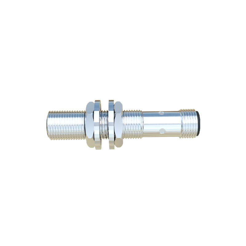
The schematic design for an inductive proximity sensor typically centers around a Colpitts or Hartley oscillator circuit, generating a high-frequency electromagnetic field from a coil (the sensor's active face). When a metallic target enters this field, eddy currents are induced, causing a change in the oscillator's amplitude or frequency. This change is detected by a subsequent demodulation and threshold circuit. The custom schematic must meticulously detail the oscillator components (coil inductance, capacitors, transistor biasing), the signal conditioning stages (amplifiers, comparators), and the output driver stage. For robust industrial use, protection circuits against short-circuits, reverse polarity, and voltage transients (e.g., using TVS diodes and series resistors) are non-negotiable and must be explicitly integrated into the schematic. Shielding techniques in the layout are crucial to prevent electromagnetic interference (EMI) from affecting the sensitive oscillator.
Capacitive sensor schematics are conceptually similar but operate on the principle of capacitance change. The sensor face and the target form a capacitor. The schematic often features an RC or LC oscillator where the sensing capacitor is part of the frequency-determining network. As a target approaches, the capacitance increases, altering the oscillation frequency. A frequency-to-voltage converter or a phase-detection circuit then processes this shift. Customization here involves calibrating the circuit's sensitivity to ignore the inherent capacitance of the sensor housing and to adjust for the dielectric constant of the target material. Schematic details must include guard ring drivers to focus the electric field and compensation networks for temperature stability.
Photoelectric sensor schematics are distinctly different, comprising three main blocks: the emitter, the receiver, and the processing logic. The emitter circuit drives an infrared LED, often with a modulated current (e.g., 5-10 kHz) to enhance noise immunity against ambient light. The receiver circuit uses a phototransistor or photodiode, followed by a high-gain amplifier tuned to the modulation frequency and a precise demodulator. The custom schematic's complexity increases for background suppression or true background suppression types, requiring precise optical alignment and analog circuitry to evaluate the angle of the reflected beam. The output stage, again, must be ruggedized for PLC compatibility.
A critical principle across all types is the design of the output interface. Whether providing a simple transistor switch (sinking or sourcing) or an analog 4-20mA/0-10V output, the schematic must include appropriate current-limiting, flyback diodes for inductive loads, and filtering. For smart sensors with digital communication (IO-Link), the schematic integrates a microcontroller or dedicated ASIC, with precise detailing of the serial interface, power supply conditioning, and ESD protection.
Power supply design within the schematic is equally vital. Most industrial sensors operate on 10-30V DC. The schematic must show a robust voltage regulator circuit, often a switching pre-regulator followed by a linear regulator for clean analog supply rails, with sufficient decoupling capacitors. Consideration for low-power or two-wire analog loop-powered designs adds another layer of schematic complexity.
Finally, the schematic is not complete without thorough annotation. Every component should have a unique reference designator, critical values (tolerance, power rating for resistors, voltage rating for capacitors) must be noted, and test points for key waveforms (oscillator signal, demodulated voltage) should be indicated. This transforms the schematic from a mere diagram into a comprehensive blueprint for prototyping, testing, and manufacturing. Adherence to these electrical and documentation principles ensures the resulting custom proximity sensor delivers reliable, repeatable performance in the demanding industrial environment for which it is engineered.