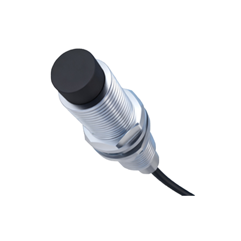
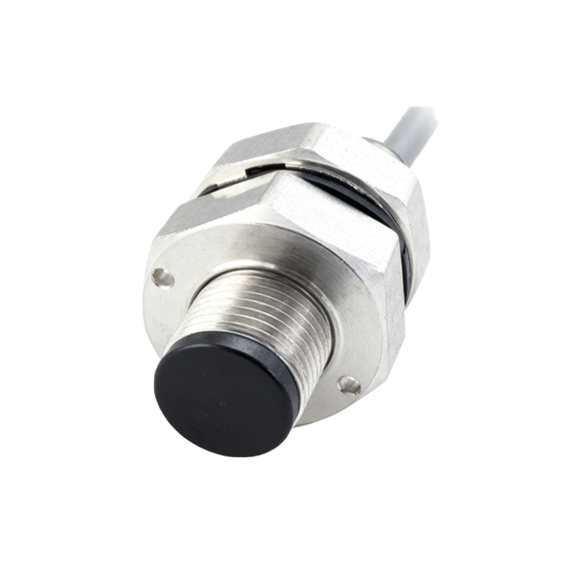
The production of Hall Effect proximity sensors represents a sophisticated intersection of semiconductor fabrication, precision assembly, and rigorous testing. These non-contact sensors, which detect the presence of nearby objects through changes in a magnetic field, are fundamental components across automotive, industrial automation, and consumer electronics. The manufacturing journey begins with the creation of the core semiconductor element—the Hall plate. This is typically fabricated on a silicon wafer using photolithography, etching, and doping processes similar to standard integrated circuit production. A thin layer of a suitable semiconductor material, often gallium arsenide (GaAs) or indium antimonide (InSb) for high sensitivity, is patterned to form the active sensing area. This plate is designed to generate a voltage differential (the Hall voltage) perpendicular to both an applied current and an external magnetic field.
Once the individual Hall plates are diced from the wafer, they proceed to packaging. This is a critical phase where the delicate semiconductor is housed within a protective casing, usually made from molded plastic or epoxy resin for standard applications, or ceramic for high-temperature or harsh environments. The package must provide mechanical protection, environmental sealing, and often includes integrated magnetic flux concentrators to enhance sensitivity. Lead frames, typically made of copper alloy, are used to connect the Hall plate's tiny bond pads to the sensor's external pins via gold or aluminum wire bonding. For more advanced sensors, the package also incorporates the necessary signal conditioning circuitry. This Application-Specific Integrated Circuit (ASIC) is either co-packaged with the Hall plate or, in monolithic designs, fabricated on the same silicon die. This circuit amplifies the microvolt-level Hall signal, provides temperature compensation, and converts it into a clean digital or analog output, such as a switched open-collector signal or a proportional voltage.
The assembly line then integrates this packaged sensor element. For many proximity sensor variants, a permanent magnet is precisely positioned relative to the Hall package. The gap and alignment between the magnet and the sensor are calibrated to define the exact switching threshold or sensing range. The entire assembly is then potted or overmolded with a robust compound to create a sealed, durable unit capable of withstanding vibration, moisture, and thermal cycling. This final housing is often engineered with specific mounting features and environmental ingress protection (IP) ratings tailored to its end-use, such as IP67 for automotive under-hood applications.
Quality control is paramount throughout the manufacturing process. Testing begins at the wafer level with probes checking the basic electrical parameters of each Hall plate. After packaging, 100% of sensors undergo automated functional testing. This involves placing each sensor in a calibrated magnetic field generated by a Helmholtz coil or a precision actuator. Test equipment verifies key parameters: the operate point (the magnetic field strength at which the sensor switches on), the release point (where it switches off), the resulting hysteresis, the output voltage levels, quiescent current consumption, and response time. Temperature cycling tests, often from -40°C to 150°C for automotive-grade sensors, ensure stability and reliability across the specified operating range. Statistical process control (SPC) monitors production data to identify and correct any process drift immediately.
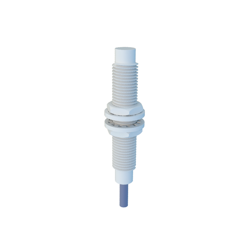
The applications dictate specific manufacturing nuances. For the automotive industry, where sensors are used for seat position detection, gearbox sensing, or brake pedal position, production follows stringent IATF 16949 quality standards. Sensors are built for high reliability over extended temperature ranges and must pass severe endurance tests. For industrial automation, where sensors detect cylinder piston position or machine part presence, the focus is on robustness, repeatability, and often on achieving very precise switching points. Consumer electronics, such as laptop lid-close detection, demand ultra-miniaturized surface-mount device (SMD) packages produced in very high volumes on fully automated pick-and-place lines.
The evolution of manufacturing technology continues to push the boundaries. Trends include the integration of more complex diagnostics and communication protocols (like IO-Link) directly into the sensor IC, the use of 3D Hall technology for sensing magnetic field direction in addition to strength, and advanced packaging techniques like wafer-level packaging (WLP) to create smaller, more cost-effective devices. The entire manufacturing chain, from crystal growth for the semiconductor wafer to the final functional test, is optimized for consistency, accuracy, and cost-efficiency, ensuring that these invisible workhorses of modern technology perform reliably in millions of critical applications every day.