In the rapidly evolving landscape of industrial automation and IoT, Bluetooth proximity sensors have emerged as a pivotal component, enabling wireless detection and data transmission. This article delves into the schematic design and operational principles of a typical Bluetooth Low Energy (BLE) based proximity sensor, tailored for engineers and technical professionals in the electrical and electronics domain.
At its core, a Bluetooth proximity sensor system integrates three fundamental modules: the sensing element, the signal conditioning and processing unit, and the BLE communication module. The schematic begins with the sensing front-end. For proximity detection, common technologies include infrared (IR), ultrasonic, or capacitive sensing. An IR-based schematic, for instance, would feature an IR LED (e.g., TSAL6200) as the emitter and a phototransistor (e.g., TEFT4300) as the receiver. The driving circuit for the LED involves a current-limiting resistor calculated based on the forward voltage and desired current. The phototransistor, typically in a common-emitter configuration, outputs a voltage signal that varies with the intensity of reflected IR light, which correlates to the presence and distance of an object.
This raw, analog signal from the sensor is often weak and noisy. Therefore, the next stage in the schematic is signal conditioning. This typically involves an operational amplifier (op-amp) circuit configured as a non-inverting amplifier or a transimpedance amplifier (for current-output sensors like photodiodes). Components like the MCP6002, a low-power op-amp, are suitable here. Following amplification, a passive RC low-pass filter is incorporated to attenuate high-frequency noise. The conditioned analog signal is then fed into the Analog-to-Digital Converter (ADC) input of a microcontroller (MCU).

The MCU serves as the brain of the system. A common choice in BLE sensor designs is a system-on-chip (SoC) that integrates both a capable MCU core and a BLE radio. Devices like the Nordic Semiconductor nRF52832 or the Texas Instruments CC2640R2F are industry standards. In the schematic, the MCU/SoC is surrounded by its essential peripheral circuitry: a stable power supply regulator (e.g., a 3.3V LDO like the MCP1700), a precise 32.768 kHz crystal oscillator for the low-speed clock, and a matching network for the main crystal (e.g., 32 MHz for the RF core). Decoupling capacitors (typically 100nF and 10µF) are placed close to the power pins of the SoC to ensure stable operation.
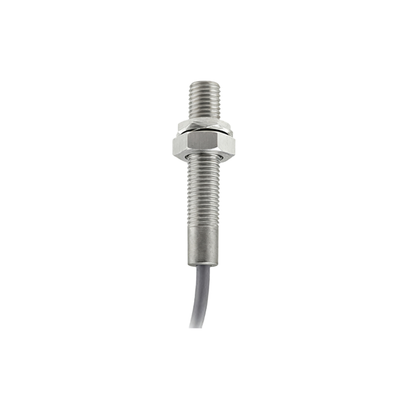
The firmware running on the MCU performs critical tasks. It reads the digitized sensor value from the ADC, applies calibration and algorithms (like a simple threshold comparison or more complex time-of-flight calculations for ultrasonic sensors) to determine proximity status (near/far) or even estimate distance. This processed data is then packaged for wireless transmission.
The BLE radio section is integral to the SoC. The schematic must include a proper antenna design and matching network to ensure regulatory compliance (FCC, CE) and optimal range. For compact designs, a chip antenna (e.g., Johanson Technology 2450AT18B100E) or a PCB trace antenna is common. The matching network, usually a Pi-network consisting of inductors and capacitors, is tuned to 2.4 GHz to maximize power transfer and minimize signal reflection. The schematic must also show the connection of the antenna's ground plane, which is crucial for radiation efficiency.
Power management is a key consideration in the schematic. Many Bluetooth proximity sensors are battery-powered. Therefore, the entire circuit is designed for ultra-low power consumption. The SoC is programmed to spend most of its time in deep sleep mode, waking up periodically to take a sensor reading and advertise or transmit data only when a state change is detected (e.g., an object comes into range). The schematic reflects this with the selection of low-quiescent-current LDOs and the configuration of GPIO pins to power down unused sensor sections.
A complete schematic also includes interfaces for programming and debugging (e.g., a Serial Wire Debug - SWD interface with connections for SWDIO and SWCLK), and possibly test points for critical signals. For user feedback, a simple LED connected via a current-limiting resistor to a GPIO pin can be included to indicate power or detection status.
In operation, the principle is straightforward yet elegant. The sensor element detects a physical change in the environment. This change is converted to an electrical signal, conditioned, digitized, and interpreted by the MCU. The MCU then uses the integrated BLE stack to format this information into a BLE advertisement packet or a connection-based data packet. These packets are transmitted via the radio front-end. A host device, such as a smartphone, industrial gateway, or PC with a BLE d