The integration of laser sensors into the Apple Watch represents a significant leap in wearable technology, merging sophisticated optical engineering with advanced signal processing. For electrical engineers, understanding the underlying principles and implementation of these sensors offers a fascinating glimpse into the future of consumer electronics and biomedical monitoring. This article delves into the technical specifics, operational mechanisms, and engineering challenges associated with the laser sensor systems found in recent Apple Watch models, particularly those used for health and environmental sensing.
At its core, the laser sensor in devices like the Apple Watch is a form of Light Detection and Ranging (LiDAR) or structured light system. It operates by emitting low-power, coherent laser light pulses toward a target—be it the user's skin for blood flow analysis or the surrounding environment for spatial mapping. The reflected or scattered light is then captured by sensitive photodetectors. The key parameter here is the time-of-flight (ToF) of each photon; by calculating the phase shift or direct time delay between the emitted and received pulses, the system can determine distance with remarkable precision, often down to the millimeter or sub-millimeter range. For electrical engineers, the design intricacies involve managing ultra-fast pulse generation, minimizing jitter in timing circuits, and ensuring the analog front-end for the photodetector has exceptionally low noise and high bandwidth.
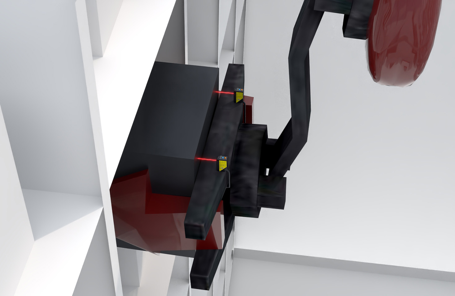
From a circuit design perspective, the laser driver is a critical component. It must deliver precise, short-duration current pulses to the laser diode to generate the optical pulses. This requires careful attention to transient response, electromagnetic interference (EMI) suppression, and thermal management, as even minor heating can shift the laser's wavelength and affect accuracy. Concurrently, the receiver chain, comprising an avalanche photodiode (APD) or a single-photon avalanche diode (SPAD) array, followed by a transimpedance amplifier (TIA) and time-to-digital converter (TDC), poses significant design challenges. Engineers must achieve a high signal-to-noise ratio (SNR) in an environment plagued by ambient light interference, motion artifacts, and the inherent quantum noise of photodetection. Advanced filtering algorithms, often implemented in dedicated digital signal processors (DSPs) or custom application-specific integrated circuits (ASICs), are employed to extract the weak return signal.
In the context of health monitoring, such as the blood oxygen (SpO2) sensing feature, the laser sensor works in concert with LEDs employing photoplethysmography (PPG). The laser provides a more focused and depth-resolved measurement compared to conventional LEDs. It can penetrate skin layers to different extents, allowing for the differentiation of arterial blood volume changes from venous and tissue background. This demands sophisticated optical modeling and calibration. The electrical design must ensure perfect synchronization between the laser emission, detector sampling, and the analog-to-digital conversion to capture the subtle plethysmographic waveform. Power management is another paramount concern; these sensors must operate within the strict energy budget of a wearable, necessitating ultra-low-power circuit design, duty cycling, and smart wake-up protocols to extend battery life without compromising data integrity.
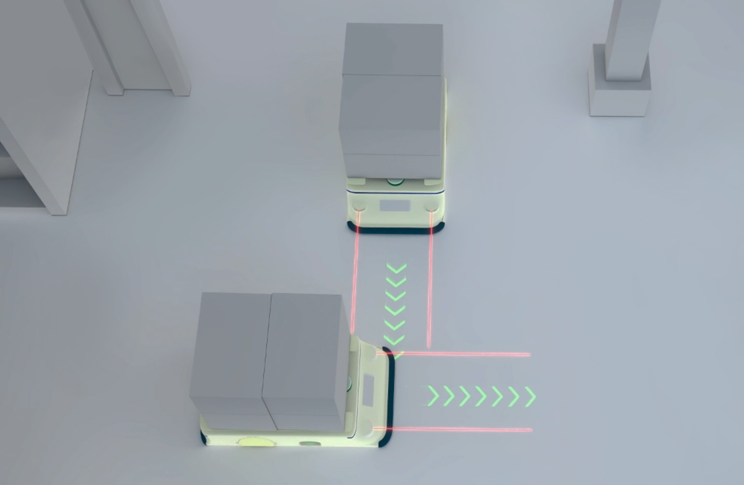
Furthermore, environmental sensing applications, like measuring distance or mapping a room, utilize the same fundamental ToF principle but often with a wider field of view. Here, the system may employ a vertical-cavity surface-emitting laser (VCSEL) array as the source. Driving a VCSEL array requires a multi-channel driver IC capable of independent channel control to support beam steering or pattern projection. The integration of these optical components with the watch's housing also presents optomechanical challenges—ensuring the laser window remains clean, free from scratches, and correctly aligned over the product's lifetime is crucial for consistent performance.
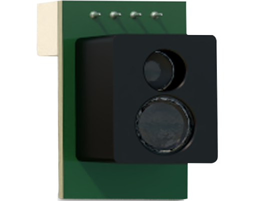
For the electrical engineering community, the Apple Watch's laser sensor is a testament to the miniaturization and integration of complex optoelectronic systems. It embodies trends in heterogeneous integration, where silicon photonics, CMOS sensor chips, and power management units are packaged into a single, compact module. Looking ahead, the evolution of these sensors points toward even higher resolution, lower power consumption, and the integration of new modalities like spectroscopic analysis. This progress will be driven by innovations in semiconductor processes, such as silicon photonics and 3D IC stacking, as well as breakthroughs in algorithmic noise reduction and sensor fusion. Understanding these systems is not only key for those developing next-generation wearables but also for engineers working in automotive LiDAR, industrial automation, and medical diagnostics, where similar principles are applied at different scales and performance requirements.