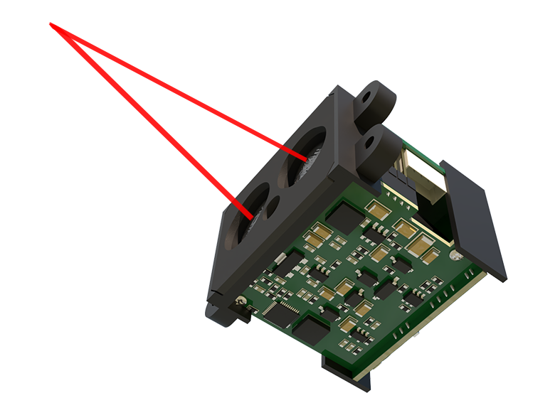
In the high-stakes world of semiconductor fabrication, precision is not merely a goal; it is the absolute foundation. Every nanometer counts, and the quality of the silicon wafer—the pristine canvas upon which integrated circuits are built—is paramount. Among the arsenal of metrology tools ensuring this quality, laser sensor scanning has emerged as a critical, non-contact technology for comprehensive wafer inspection and measurement. This process involves directing a focused, coherent laser beam across the wafer surface to capture detailed topographical and dimensional data with exceptional speed and accuracy.
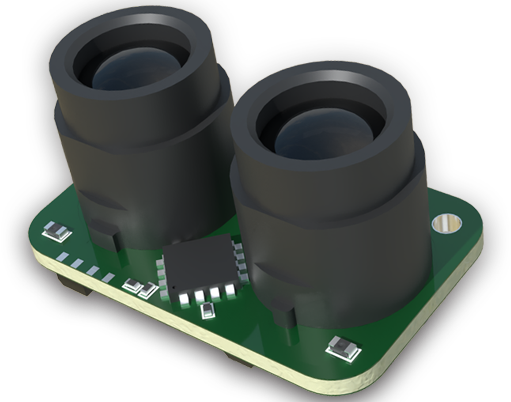
The core principle relies on triangulation or interferometry. In a common triangulation setup, a laser diode projects a precise spot or line onto the wafer. A high-resolution CMOS or CCD sensor, positioned at a known angle, captures the reflection. Any variation in the wafer's surface height causes a displacement of the laser point in the sensor's field of view. Sophisticated algorithms then translate this displacement into precise Z-axis height data, building a detailed three-dimensional map of the wafer as the scanner or wafer stage moves. For even higher precision applications, laser interferometers are used, measuring the phase shift of the reflected laser light to detect sub-nanometer variations.
The applications of laser scanning within the wafer manufacturing and processing lifecycle are extensive. First, in incoming wafer inspection, lasers rapidly scan for global shape parameters like bow, warp, and total thickness variation (TTV). Identifying these macro-scale defects early prevents costly processing of substandard substrates. During the front-end-of-line (FEOL) processes, such as chemical-mechanical planarization (CMP), laser scanners provide real-time, in-situ monitoring of film thickness and planarity uniformity across the wafer. Post-etch and post-lithography, they are indispensable for critical dimension (CD) measurement and for detecting pattern defects, residues, or microroughness that could impair device performance.
Furthermore, laser sensor scanning plays a vital role in overlay metrology, ensuring successive lithography layers are aligned with near-atomic precision. By scanning specialized overlay marks, the system can detect misalignment errors that, if uncorrected, would render the circuitry non-functional. The technology is also crucial for backside inspection, identifying particles or scratches that could cause thermal or mechanical issues during packaging.
The advantages over traditional contact methods like stylus profilometers are significant. The non-contact nature eliminates the risk of surface damage or contamination on the delicate wafer. Laser scanning offers vastly superior speed, enabling 100% inspection or high-density sampling that would be impractical with slower techniques. It provides full-field 3D data rather than single line profiles, giving a more complete picture of surface morphology. The data is digital and immediately available for statistical process control (SPC), allowing for rapid feedback and adjustment of fabrication tools to maintain yield.
However, the implementation of laser sensor scanning is not without challenges. Highly reflective or transparent film stacks can cause signal noise or penetration issues, requiring specialized sensor configurations or algorithms. The presence of intricate, high-aspect-ratio patterns can create shadowing effects, limiting the sensor's ability to probe certain features. As device nodes shrink to 3nm and below, the requirements for measurement precision and repeatability push laser technology to its physical limits, often necessitating hybrid metrology approaches that combine laser data with information from other sources like scatterometry or atomic force microscopy.
Looking forward, the evolution of laser sensor technology is tightly coupled with the semiconductor industry's roadmap. Trends point towards faster scan rates to keep pace with high-throughput manufacturing, the use of shorter wavelength lasers for improved lateral resolution, and enhanced data analytics powered by machine learning. AI-driven algorithms can learn to distinguish critical defects from harmless noise more effectively, predicting process drift before it impacts yield. Furthermore, the integration of laser scanners into clustered process tools for closed-loop control represents the next frontier in smart manufacturing.
In conclusion, laser sensor scanning is a cornerstone of modern semiconductor metrology. It provides the essential eyes for the manufacturing process, delivering the high-speed, non-contact, and precise dimensional data required to produce the advanced chips that power today's technology. As wafers grow larger (transitioning to 450mm) and features continue to shrink, the role of advanced laser scanning will only become more central to maintaining the relentless pace of innovation and the economic viability of semiconductor production.