In the rapidly evolving landscape of industrial automation, metrology, and quality control, the physical size of sensing components has become a critical design parameter. Laser displacement sensors, renowned for their high precision and non-contact measurement capabilities, are undergoing a significant trend toward miniaturization. This article delves into the factors driving the reduction in sensor volume, the technological advancements enabling compact designs, and the practical implications for system integration and application versatility.
The push for smaller laser displacement sensors is primarily driven by space constraints in modern manufacturing and assembly lines. As robotic cells become more densely packed and production machinery more complex, the available real estate for mounting inspection devices is severely limited. A bulky sensor can interfere with moving parts, limit the range of motion of robotic arms, or simply be impossible to install in intricate assemblies. Consequently, sensor manufacturers are relentlessly pursuing reductions in the overall footprint and profile of their laser displacement units without compromising the core performance metrics of accuracy, repeatability, and measurement range.
Technologically, this miniaturization is made possible by several key innovations. First, advancements in laser diode and lens technology have allowed for the creation of highly collimated, stable laser beams from extremely small emitter packages. Modern semiconductor lasers are not only smaller but also more efficient, generating less heat, which in turn reduces the need for large heat sinks within the sensor housing. Second, the miniaturization of CMOS and CCD imaging sensors plays a pivotal role. The receiver unit, which captures the laser spot, can now be fabricated on a microscopic scale while maintaining high resolution and fast sampling rates. Third, the integration of powerful application-specific integrated circuits (ASICs) and system-on-chip (SoC) designs consolidates signal processing, communication protocols, and sometimes even basic logic functions into a single, tiny electronic component. This eliminates the need for separate, space-consuming circuit boards.
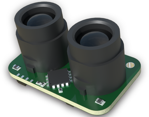
The evolution of housing materials and mechanical design also contributes significantly. The use of high-strength, lightweight alloys and advanced engineering polymers allows for robust yet slim enclosures. Innovative optical designs, such as folded light paths or the use of micro-prisms within the sensor body, enable a longer effective optical path within a shorter physical housing, which is crucial for triangulation-based sensors. Furthermore, the shift toward integrated connectivity, like M8/M12 connectors instead of larger terminal blocks, and the adoption of industry-standard compact form factors (e.g., "pencil-type" sensors) have standardized the push for smaller volumes.
The benefits of this compact design revolution are manifold. For system integrators and machine builders, smaller sensors offer unparalleled flexibility. They can be installed in previously inaccessible locations—inside narrow pipes, on small end-effectors of collaborative robots, or within compact inspection jigs. This enables more measurement points per machine, leading to richer data and more comprehensive quality assurance. The reduced weight is also a boon for dynamic applications on moving gantries or robot wrists, minimizing inertia and vibration issues. From a logistical standpoint, smaller sensors are easier to inventory, handle, and ship.
However, the journey toward miniaturization is not without its challenges and trade-offs. A primary concern is heat dissipation. Packing high-performance electronics into a tiny space increases power density, which can lead to thermal drift—a change in measurement output due to temperature fluctuations. Manufacturers combat this through sophisticated thermal management designs, low-power electronics, and software-based temperature compensation algorithms. Another potential trade-off is in the maximum measurement range or spot size; a very compact sensor might have a slightly shorter working distance compared to a larger counterpart with a more powerful laser and larger lens assembly. Users must therefore carefully evaluate their specific application requirements against the sensor's specifications.
Looking ahead, the trend toward miniaturization in laser displacement sensors is expected to continue, fueled by demands from emerging fields like micro-electronics assembly, precision medical device manufacturing, and additive manufacturing. The convergence of photonics, nanotechnology, and advanced materials science promises even smaller, perhaps even chip-scale, laser measurement devices in the future. For engineers and technicians, understanding the principles behind sensor volume and its relationship to performance is essential for selecting the right tool. The ideal sensor is no longer just about the highest specification on paper, but the one that delivers reliable precision in the smallest possible form factor, seamlessly integrating into the smart, compact, and agile factories of tomorrow.