In the realm of industrial automation and process control, laser level sensors have emerged as a critical technology for precise, non-contact measurement. The manufacturing of these sophisticated devices is a complex, multi-stage process that demands high precision, stringent quality control, and deep expertise in optics, electronics, and materials science. This guide delves into the core aspects of laser level sensor production, from initial design to final calibration.
The journey begins with the design and engineering phase. This stage involves defining the sensor's specifications, such as measurement range, accuracy, response time, and the type of laser source—typically a Class 2 laser diode for safety and reliability. Engineers use advanced CAD and simulation software to model the optical path, ensuring the laser beam is correctly focused and the receiver optics are optimally positioned to capture the reflected signal. The housing design is equally crucial, as it must protect sensitive internal components from harsh industrial environments, including dust, moisture, vibration, and extreme temperatures. Material selection, often involving robust polymers or stainless steel, is finalized here.
Following design, the procurement of high-quality components is paramount. The heart of the sensor is the laser diode module, chosen for its wavelength (commonly 650nm red or 850nm infrared), output power, and beam characteristics. Complementary Metal-Oxide-Semiconductor (CMOS) or Position-Sensitive Detector (PSD) chips are selected as the receiving elements for their sensitivity and speed. Printed Circuit Board (PCB) fabrication is initiated, incorporating microcontrollers, signal conditioning circuits, and communication interfaces (e.g., 4-20mA, RS485, IO-Link). All components must be sourced from reliable suppliers with certifications to ensure consistency and longevity.
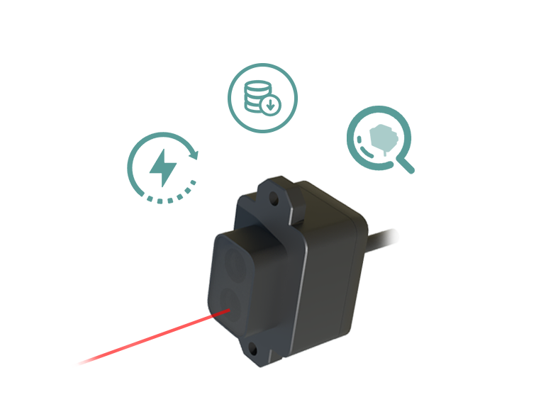
The core manufacturing process is assembly, conducted in controlled cleanroom environments to prevent contamination. The process is typically a combination of automated precision and skilled manual work. Automated pick-and-place machines populate the PCB with surface-mount devices (SMDs). The populated PCB then undergoes reflow soldering in an oven, creating secure electrical connections. In parallel, the mechanical assembly takes place. The laser diode and receiver optics are meticulously aligned and secured within the sensor housing. This optical alignment is a critical step, often performed using specialized fixtures and microscopes, as even micron-level misalignment can drastically affect measurement accuracy. The PCB is then integrated, and all internal wiring is connected.
Once assembled, the sensor enters the programming and calibration phase. Firmware is loaded onto the microcontroller. This software governs the sensor's operation, including laser pulse generation, signal processing algorithms for noise filtering, and the calculation of distance based on time-of-flight or phase-shift principles. Calibration is the most critical quality step. Each sensor is tested against known reference distances in a controlled setup. Calibration parameters are adjusted to ensure the output signal linearly and accurately corresponds to the actual level. This process often involves temperature cycling to compensate for thermal drift, ensuring stable performance across the specified operating range.
Rigorous testing and quality assurance follow calibration. Sensors undergo a battery of tests simulating real-world conditions. These include accuracy verification across the full measurement range, long-term stability tests, ingress protection (IP) rating tests for dust and water resistance, electromagnetic compatibility (EMC) tests, vibration and shock tests, and checks for compliance with laser safety standards (IEC 60825-1). Any unit failing any test is rejected or sent for rework. Only sensors passing all criteria proceed to final packaging.
The final stage involves labeling, documentation, and packaging. Each sensor is labeled with a unique serial number for traceability. Comprehensive documentation, including datasheets, installation manuals, and safety certificates, is prepared. Packaging is designed to protect the sensor during shipping and storage.
The manufacturing of laser level sensors is a testament to precision engineering. It requires a seamless integration of optical design, electronic miniaturization, robust mechanical construction, and intelligent software. As industries demand higher accuracy and reliability for applications in silo monitoring, liquid tank management, and bulk solid level detection, manufacturers continue to innovate in production techniques, adopting more automation for consistency and exploring new materials and laser technologies to enhance performance and durability. The end goal is always to deliver a sensor that provides trustworthy, maintenance-free measurement in the most demanding environments.