In industrial automation and motion control systems, laser speed sensors play a critical role in providing non-contact, high-precision velocity measurements. The underlying electronic circuit is the core that enables this functionality. This article delves into the typical circuit diagram of a laser Doppler velocimetry (LDV) sensor, explaining key components and their operational principles.
A standard laser speed sensor circuit can be broadly divided into several functional blocks: the laser diode driver, the optical receiver front-end, the signal conditioning and processing unit, and the output interface.
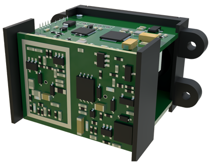
The circuit begins with a stable laser source. A constant current laser diode driver circuit is essential. This circuit typically uses a precision operational amplifier in a feedback loop with a current-sensing resistor and a field-effect transistor (FET) to regulate the current through the laser diode. Thermal compensation circuits, often involving a thermistor network and a separate control loop, are integrated to maintain wavelength stability, as temperature fluctuations directly impact measurement accuracy.
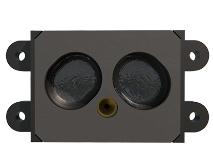
The heart of the measurement lies in the optical receiver. Photodetectors, commonly avalanche photodiodes (APDs) or high-speed PIN photodiodes, convert the back-scattered laser light (which has undergone a frequency shift proportional to the target's velocity) into a weak electrical current signal. This photocurrent is extremely small, necessitating a high-gain, low-noise transimpedance amplifier (TIA) as the first stage. The TIA's feedback resistor and capacitor values are carefully selected to achieve the necessary bandwidth while minimizing noise. Following the TIA, AC coupling blocks any DC component from ambient light.
The resulting signal contains the Doppler frequency shift. The next stage involves signal conditioning. Band-pass filters are employed to isolate the frequency range of interest from noise. For sensors dealing with very low speeds, the Doppler frequency can be in the kHz or even Hz range, requiring filters with very sharp roll-off characteristics. Subsequently, the signal is amplified further by a variable-gain amplifier (VGA) to ensure optimal amplitude for the processing stage.
Signal processing is performed by a high-speed comparator or a specialized mixed-signal IC. The comparator converts the analog signal into a digital square wave. The frequency of this wave is directly proportional to the target speed. A microcontroller unit (MCU) or a digital signal processor (DSP) then measures this frequency using high-resolution timer/counter peripherals. Advanced sensors implement Fast Fourier Transform (FFT) algorithms in the DSP to handle complex signal patterns or multiple targets. The MCU/DSP calculates the velocity using the known laser wavelength and the optical geometry of the system (v = f * λ / (2 * cosθ)).
Finally, the output interface circuit provides the measured data. This often includes digital outputs like RS-485, CAN bus, or Ethernet for industrial networks, and analog outputs such as 4-20 mA or 0-10 V for direct connection to PLCs. Each output type requires specific driver circuits: line drivers for RS-485, CAN transceivers, or digital-to-analog converters (DACs) with voltage/current buffers for analog outputs.
Power management is crucial throughout. The circuit requires multiple regulated voltage rails (e.g., ±5V, ±12V, 3.3V) for analog and digital sections. Low-dropout regulators (LDOs) and switch-mode power supplies (SMPS) with proper filtering are used to prevent switching noise from interfering with sensitive analog measurements.
Designing such a circuit demands careful attention to noise reduction. Techniques include using multilayer PCBs with separate ground planes for analog and digital sections, strategic component placement, and extensive use of decoupling capacitors. Shielding the photodetector and front-end amplifier from electromagnetic interference (EMI) is also paramount.
In summary, the laser speed sensor circuit is a sophisticated integration of precision analog design, high-speed digital processing, and robust industrial interfacing. Understanding each block's role within the complete schematic is key to developing, maintaining, and troubleshooting these vital industrial measurement tools.