In the realm of laser sensor technology, the concept of minimum spot size is a critical parameter that directly influences measurement accuracy, resolution, and overall system performance. This article delves into the principles, factors, and applications associated with achieving the smallest possible laser spot in sensor designs, tailored for professionals in the electrical and instrumentation industries.
Laser sensors operate by emitting a focused beam of light onto a target surface, with the reflected or scattered light being detected to determine properties such as distance, position, or surface characteristics. The spot size refers to the diameter of the laser beam at its point of contact with the target. A smaller spot size enables higher spatial resolution, allowing for precise detection of fine features and edges, which is essential in applications like semiconductor inspection, precision machining, and biomedical imaging.
The minimum achievable spot size is governed by fundamental optical principles, primarily diffraction limits as described by the Rayleigh criterion. According to this, the spot size is proportional to the wavelength of the laser light and inversely proportional to the numerical aperture (NA) of the focusing optics. In mathematical terms, the diffraction-limited spot diameter (d) can be approximated as d ≈ 1.22 * λ / NA, where λ is the wavelength. This implies that shorter wavelengths (e.g., ultraviolet or blue lasers) and higher NA lenses can produce smaller spots. For instance, using a laser with a wavelength of 405 nm and an objective lens with an NA of 0.95, one can achieve spot sizes below 1 micrometer, enhancing resolution for micro-scale measurements.
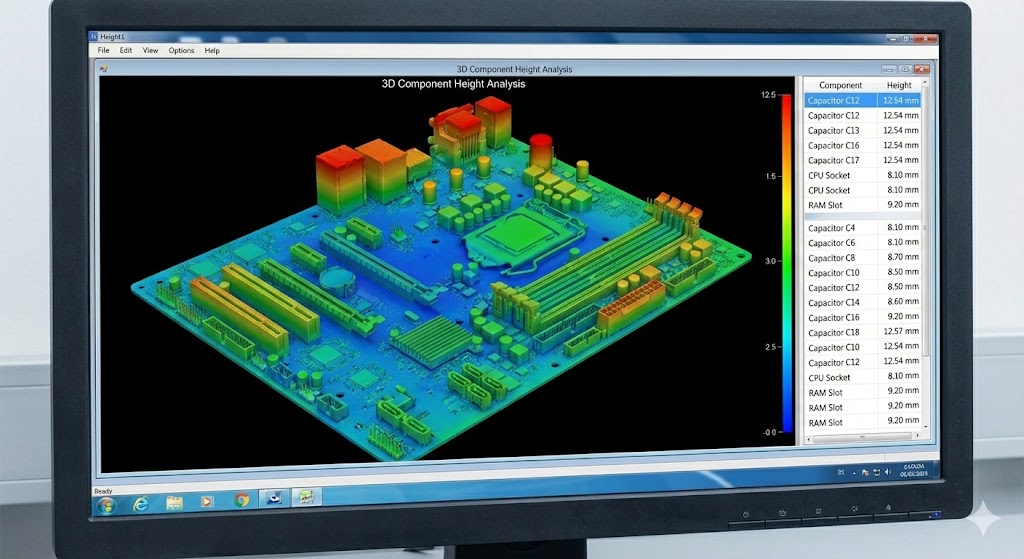
Several factors impact the practical realization of minimum spot size in laser sensors. First, laser beam quality, characterized by the M² factor, plays a significant role. An ideal Gaussian beam (M² = 1) allows for tight focusing, while deviations due to aberrations or multimode operation can enlarge the spot. High-quality single-mode lasers are often preferred to minimize this effect. Second, optical components such as lenses and mirrors must be precisely aligned and free from defects to avoid aberrations like spherical or chromatic distortion, which can degrade spot quality. Third, environmental conditions, including temperature fluctuations and vibrations, can cause thermal drift or mechanical misalignment, affecting spot stability. Engineers must account for these in sensor design through robust housing and calibration techniques.
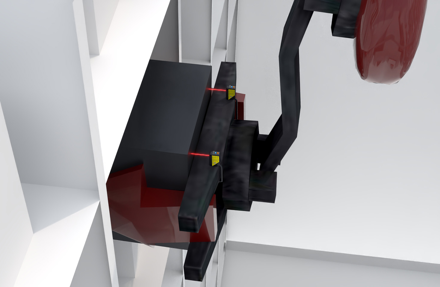
In industrial applications, achieving a small laser spot is paramount for tasks requiring high precision. For example, in laser triangulation sensors used for displacement measurement, a smaller spot reduces measurement uncertainty on rough or inclined surfaces, improving accuracy to sub-micron levels. Similarly, in confocal microscopy sensors, minimal spot size enhances axial resolution, enabling detailed 3D profiling of materials. However, challenges arise when dealing with diffusive or transparent targets, where scattering or refraction can distort the spot. Advanced techniques like adaptive optics or computational algorithms are employed to compensate for such issues, ensuring reliable performance.
Recent advancements in laser sensor technology have pushed the boundaries of minimum spot size. Innovations in fiber lasers, photonic crystal fibers, and diffractive optical elements allow for more compact and efficient focusing systems. Additionally, the integration of artificial intelligence for real-time spot optimization is gaining traction, enabling adaptive control based on target properties. As industries move towards miniaturization and higher precision, the demand for sensors with ultra-small spot sizes is expected to grow, driving further research in nanophotonics and quantum optics.
To summarize, the minimum spot size in laser sensors is a key determinant of measurement fidelity, rooted in optical physics and influenced by design and environmental factors. By leveraging short-wavelength lasers, high-NA optics, and quality components, engineers can achieve spots on the order of micrometers or less, catering to demanding applications across manufacturing, healthcare, and research. Continuous innovation in this area promises to enhance sensor capabilities, paving the way for next-generation inspection and metrology systems.