In the realm of high-precision measurement and industrial automation, the pursuit of accuracy is relentless. Among the most critical tools enabling this pursuit are laser displacement sensors, particularly those boasting resolutions as fine as 0.0001mm. This level of precision, often referred to as sub-micron or even nanometer-level measurement, represents the pinnacle of non-contact sensing technology. It fundamentally transforms quality control, process monitoring, and R&D across industries from semiconductor manufacturing to advanced optics and aerospace engineering.
The core principle behind a laser displacement sensor is triangulation. A focused laser beam is projected onto the target surface. The reflected light is then captured by a high-resolution receiving element, typically a CCD or CMOS linear array. Any minute change in the distance to the target causes a proportional shift in the position of the laser spot on this receiver. By analyzing this shift with sophisticated algorithms, the sensor calculates the displacement with extreme accuracy. Achieving a stable 0.0001mm resolution demands excellence at every stage of this process: an ultra-stable laser diode with a perfectly defined wavelength, precision optics to shape and focus the beam, a high-sensitivity receiver with minimal noise, and advanced signal processing electronics capable of filtering out environmental interference.
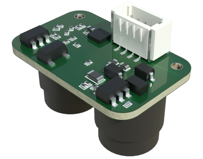
The specification of 0.0001mm is not merely a number; it defines a sensor's capability to detect variations invisible to the human eye and beyond the reach of conventional contact probes. This capability is paramount in applications where surface finish, flatness, or dimensional tolerances are critical. For instance, in the production of semiconductor wafers, measuring wafer thickness, warp, and bow with such precision ensures the integrity of microchips. In precision machining, it allows for real-time monitoring of tool wear and part dimensions during high-speed milling or grinding, preventing costly scrap and rework. Furthermore, in the assembly of micro-electromechanical systems (MEMS) or optical components, these sensors enable the alignment and gap control necessary for device functionality.
However, harnessing this level of precision requires a deep understanding of the sensor's operating conditions and limitations. Factors that might be negligible for lower-resolution sensors become significant challenges. Environmental stability is crucial. Thermal fluctuations can cause material expansion or contraction, affecting both the sensor and the target. Vibrations must be minimized or compensated for, as they can introduce noise into the measurement signal. The characteristics of the target surface itself are also critical. While modern sensors can handle a variety of materials, highly reflective, transparent, or absorptive surfaces may require specific models with adjustable laser power or specialized optical filters to ensure a reliable return signal. Proper installation, calibration against a known standard, and periodic verification are non-negotiable practices to maintain stated accuracy.
The integration of a 0.0001mm-resolution laser sensor into an automated system involves more than just mounting the unit. It necessitates a holistic approach to system design. This includes selecting rigid and thermally stable mounting structures, implementing environmental enclosures if necessary, and ensuring data acquisition systems have sufficient sampling rates and bit depth to fully utilize the sensor's output. The data generated is often fed into statistical process control (SPC) software, enabling trend analysis and predictive maintenance, thus moving from simple inspection to proactive process optimization.
Looking forward, the evolution of laser displacement sensing continues. Advancements in blue laser technology offer better performance on certain materials, while multi-point and profile sensors are expanding from single-point distance measurement to capturing complex surface topographies with the same high resolution. The integration with AI and machine learning for automated defect recognition and classification is another growing frontier. The 0.0001mm laser displacement sensor, therefore, is not an endpoint but a key enabler in the ongoing journey toward smarter, more precise, and more efficient manufacturing and research. It embodies the convergence of optics, electronics, and software engineering, providing the foundational data that drives innovation and ensures excellence in the most demanding technical applications.