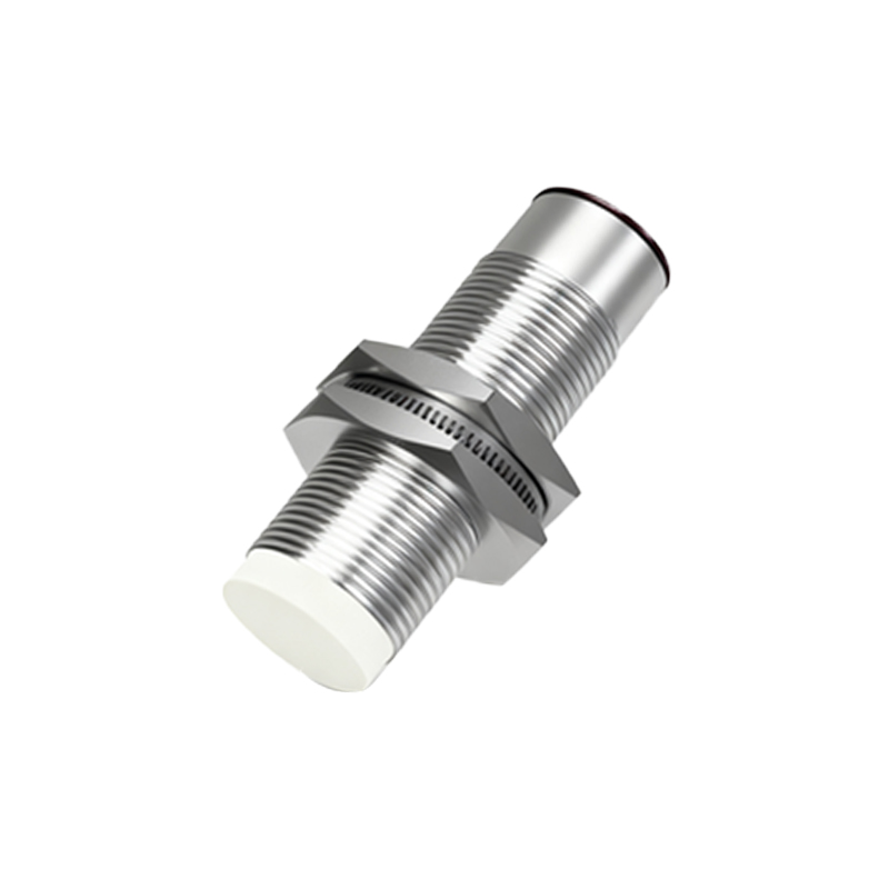
The relentless drive towards smaller, more integrated electronic devices has placed immense pressure on component manufacturers to miniaturize. Among these components, proximity sensors present a unique set of design challenges. Their function—to detect the presence or absence of an object within a defined range without physical contact—is fundamentally tied to their physical architecture. Simply shrinking a traditional sensor design often leads to a significant degradation in performance, making miniaturization a complex engineering endeavor that balances size, power, sensitivity, and reliability.
One of the primary hurdles in micro proximity sensor design is maintaining adequate sensing range and signal integrity. The sensing field strength of inductive or capacitive sensors is directly related to the size and geometry of their coils or electrodes. A reduction in physical size typically weakens this field, shortening the effective detection distance. Engineers combat this through advanced coil winding techniques, using higher-permeability core materials, and optimizing the oscillator circuit design to maximize efficiency. For optical proximity sensors, the challenge lies in fitting the infrared LED and photodetector into a tiny footprint while preventing optical crosstalk. Innovative solutions include molded lens packages that precisely direct light and sophisticated shielding structures built directly into the housing.
Power consumption becomes a critical constraint in miniature designs, especially for battery-powered devices like wearables and IoT sensors. A smaller device often means a smaller battery. Designers must therefore create ultra-low-power systems. This involves selecting components with minimal quiescent current, implementing aggressive power management schemes where the sensor sleeps most of the time and only wakes at precise intervals, and optimizing the sensing algorithm for speed. The goal is to achieve the necessary measurement with the shortest possible active time. Advances in low-power ASICs (Application-Specific Integrated Circuits) that integrate the analog front-end, digital logic, and communication interface into a single chip are pivotal in reducing overall system power.
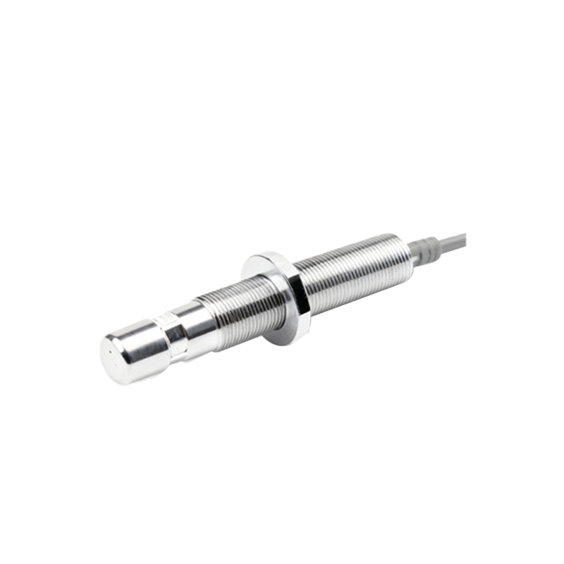
Integration and packaging are perhaps the most visible aspects of miniaturization. The trend is moving decisively away from discrete components on a PCB towards fully integrated modules. System-in-Package (SiP) technology allows for the combination of the sensor die, a microcontroller, and even a radio chip into one compact, surface-mount package. This not only saves space but also improves performance by shortening signal paths and reducing electromagnetic interference. However, this high level of integration generates new concerns, primarily thermal management and mechanical stress. The heat generated by the ICs in a tightly sealed package must be effectively dissipated to prevent drift in sensor calibration. Furthermore, the package must protect delicate MEMS (Micro-Electro-Mechanical Systems) elements, common in some proximity sensors, from stresses induced by soldering and daily use.
Environmental robustness cannot be sacrificed for size. A micro proximity sensor destined for an automotive, industrial, or outdoor application must withstand temperature extremes, humidity, vibration, and contamination. Achieving this in a tiny form factor requires novel materials and sealing techniques. Conformal coatings, gel filling, and laser-welded housings are employed to create hermetic seals. The design must also account for electromagnetic compatibility (EMC); a smaller sensor is more susceptible to noise from nearby radios or power supplies, necessitating careful PCB layout and filtering within the integrated circuit itself.
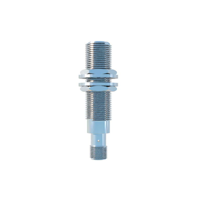
The application landscape for these miniature sensors is vast and growing. They are the enabling technology for smartphone display blanking during calls, touchless interfaces in smart home devices, lid detection in laptops, and presence detection in ultra-compact industrial equipment. In medical devices, tiny proximity sensors ensure proper alignment or detect fluid levels. The future points toward even greater integration, with sensors being embedded directly into flexible substrates or the casings of devices themselves, becoming virtually invisible. Success in this field requires a multidisciplinary approach, merging expertise in semiconductor physics, analog and digital circuit design, materials science, and advanced packaging. The journey of proximity sensor miniaturization is a continuous pursuit of the optimal equilibrium point where microscopic size meets macroscopic functionality.