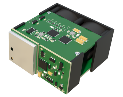
In the realm of precision measurement and control, a transformative technology is steadily gaining prominence: the monolithic laser sensor. Unlike traditional sensor assemblies that integrate discrete components like lasers, photodetectors, and optics from various sources, a monolithic laser sensor is fabricated from a single, continuous piece of semiconductor material, typically indium phosphide or gallium arsenide. This fundamental architectural shift from a hybrid to an integrated system unlocks a new echelon of performance, reliability, and miniaturization, making it a cornerstone for next-generation industrial and scientific applications.
The core advantage lies in its inherent structural integrity. By etching the laser cavity, waveguides, modulators, and detection elements directly onto a single chip, the sensor eliminates the need for delicate optical alignments and numerous mechanical interfaces. In conventional setups, thermal expansion, mechanical vibrations, and long-term wear can misalign optical components, leading to signal drift, calibration errors, and eventual failure. A monolithic design renders the sensor virtually immune to these issues. The optical path is permanently and precisely defined during fabrication, ensuring exceptional long-term stability. This robustness is invaluable in harsh environments such as factory floors with significant vibration, automotive under-hood applications with wide temperature swings, or remote field deployments where maintenance is impractical.
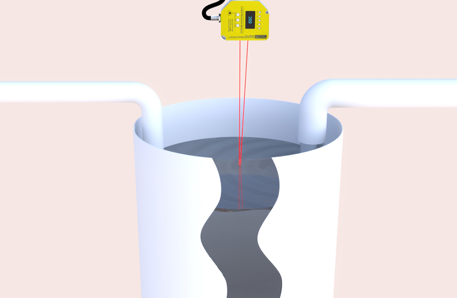
This integration directly translates to superior performance metrics. The close proximity of components on the chip minimizes optical loss and parasitic effects, allowing for higher signal-to-noise ratios and greater sensitivity. Furthermore, the co-integration of active laser elements with passive or active optical components enables sophisticated on-chip signal processing. For instance, frequency modulation or wavelength tuning can be achieved directly within the chip architecture, facilitating techniques like frequency-modulated continuous-wave (FMCW) LiDAR for precise distance and velocity measurement without moving parts. This leads to sensors capable of sub-micron resolution in displacement measurement, part-per-billion sensitivity in gas concentration detection, or ultra-fast, jitter-free timing for synchronization applications.
Miniaturization is another compelling benefit. The entire sensor system can be packaged into a chip-scale device, often just a few millimeters in size. This small footprint enables integration into spaces previously inaccessible to bulkier sensor modules. It is a critical enabler for portable analytical instruments, wearable health monitors, and dense sensor networks for the Internet of Things (IoT). The reduced size and weight are particularly crucial in aerospace and mobile robotics, where every gram matters.
From an economic and manufacturing perspective, monolithic integration promises scalability. While the initial design and mask creation are complex, the subsequent wafer-scale fabrication process is highly parallelizable, similar to semiconductor chip production. This potential for mass production can significantly drive down unit costs over time, making high-performance laser sensing accessible for high-volume applications like consumer electronics and automotive LiDAR systems. The reliability stemming from fewer parts also reduces lifetime costs associated with calibration, downtime, and replacement.
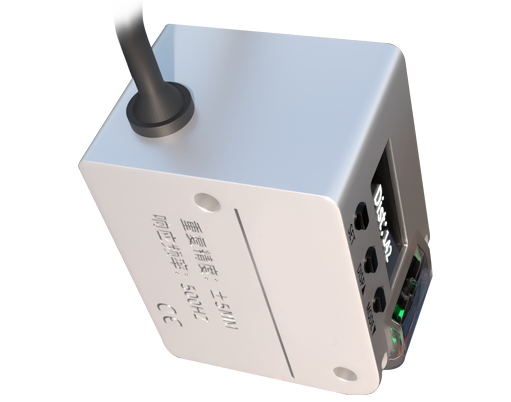
The applications for monolithic laser sensors are vast and expanding. In industrial automation, they provide non-contact, high-speed measurement for quality control, wafer inspection, and robotic guidance. In environmental monitoring, integrated photonic chips can be deployed as compact, low-power spectral analyzers to detect trace gases or pollutants. The telecommunications industry leverages them for ultra-stable reference oscillators and signal monitoring. In biomedical devices, they enable miniaturized flow cytometers, optical coherence tomography (OCT) probes, and lab-on-a-chip diagnostic systems. The advent of autonomous vehicles heavily relies on solid-state, reliable LiDAR, where monolithic laser sensor arrays are a key technology for creating compact, durable, and cost-effective 3D perception systems.
Despite the clear advantages, challenges remain. The design and fabrication of these photonic integrated circuits require specialized foundries and expertise, which can create barriers to entry. Coupling light efficiently from the tiny chip to the external world (optical fiber or free space) still presents an engineering hurdle. However, ongoing research in packaging, silicon photonics hybrid integration, and standardized photonic component libraries is rapidly addressing these obstacles.
In conclusion, monolithic laser sensors represent a paradigm shift, moving laser-based sensing from the domain of assembled instruments to that of integrated semiconductor devices. By offering unmatched stability, enhanced performance, radical miniaturization, and a path to low-cost volume production, they are poised to become the default solution for an ever-widening array of precision measurement challenges. As fabrication technologies mature and design tools improve, their influence will permeate deeper into industry, science, and daily life, enabling smarter, more responsive, and more efficient systems across the board.