Introduction to GaAs Photodetectors
Gallium Arsenide (GaAs) has established itself as a cornerstone material in the realm of optoelectronics, particularly for photodetection. Its intrinsic properties, such as a direct bandgap of approximately 1.42 eV at room temperature and high electron mobility, make it exceptionally suitable for detecting light in the near-infrared and visible spectrum. Unlike silicon, GaAs can efficiently absorb photons and convert them into electrical signals without the need for an indirect bandgap phonon-assisted process, leading to higher quantum efficiency and faster response times. This fundamental advantage underpins the widespread adoption of GaAs-based photodetectors in high-speed and high-sensitivity applications.

Fundamental Operating Principles
The core operation of a GaAs photodetector relies on the photoelectric effect within the semiconductor. When photons with energy greater than the bandgap energy of GaAs strike the device, they excite electrons from the valence band to the conduction band, generating electron-hole pairs. These photogenerated carriers are then swept by an internal or external electric field, creating a measurable photocurrent. Common device structures include p-i-n photodiodes, metal-semiconductor-metal (MSM) photodetectors, and avalanche photodiodes (APDs). Each structure offers distinct trade-offs between responsivity, bandwidth, dark current, and operational voltage, allowing engineers to tailor the device to specific system requirements.
Key Material and Structural Advantages
The superiority of GaAs stems from its material science. Its direct bandgap enables the fabrication of thin, yet highly absorbing active layers, which is crucial for achieving high-speed performance by minimizing carrier transit time. Furthermore, GaAs can be lattice-matched with other III-V compound semiconductors like AlGaAs and InGaAs, enabling the creation of sophisticated heterostructures. These heterojunctions can be engineered to form separate absorption and multiplication regions in APDs or to create resonant-cavity-enhanced detectors for wavelength-selective applications. The ability to integrate monolithically with GaAs-based electronic circuits also paves the way for compact optoelectronic integrated circuits (OEICs).
Primary Application Domains
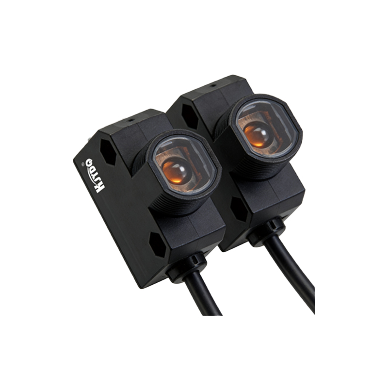
GaAs photodetectors are indispensable in several cutting-edge fields. In fiber-optic communications, they serve as high-speed receivers in systems operating at 850 nm and 1300 nm windows, enabling data transmission at gigabits-per-second rates. In sensing and metrology, they are used in laser rangefinders, LIDAR systems for autonomous vehicles, and precision analytical instruments. The defense and aerospace sectors utilize them in missile guidance, secure free-space optical communication, and infrared countermeasures. Their fast response also makes them ideal for time-resolved spectroscopy and quantum key distribution systems.
Performance Metrics and Design Considerations
Evaluating a GaAs photodetector involves several critical parameters. Responsivity (A/W) measures the electrical output per optical input. Bandwidth, determined by the RC time constant and carrier transit time, defines the maximum operational speed. Dark current, the noise current in the absence of light, directly impacts the signal-to-noise ratio and the minimum detectable power. Quantum efficiency indicates the percentage of incident photons that generate charge carriers. Designers must carefully balance these metrics, often optimizing the doping profile, absorption layer thickness, and electrode geometry to meet the specific demands of bandwidth, sensitivity, and dynamic range.
Current Challenges and Research Frontiers
Despite their maturity, GaAs photodetectors face ongoing challenges. Reducing dark current, especially in APDs operating near breakdown voltage, remains a key focus to improve sensitivity. Extending the spectral response further into the near-infrared, where InGaAs dominates, is an area of active research through bandgap engineering with ternary and quaternary alloys. Another frontier involves integrating GaAs photodetectors on silicon substrates to combine the optoelectronic prowess of III-V materials with the vast, low-cost silicon CMOS manufacturing ecosystem, a significant step towards large-scale photonic integration.
Future Outlook and Conclusion
The future of GaAs-based photodetection is intertwined with advancements in material growth, nanofabrication, and system integration. Emerging concepts like plasmonic enhancement, which uses nanostructures to concentrate light and enhance absorption, promise to break traditional performance limits. The development of single-photon avalanche diodes (SPADs) based on GaAs materials will be crucial for quantum information technologies and ultra-weak light detection. As the demand for higher bandwidth, greater sensitivity, and more compact systems grows across telecommunications, sensing, and computing, GaAs photodetectors will continue to evolve, solidifying their role as a vital enabling technology in the photonic age.