Proximity sensors are fundamental components in modern industrial automation, robotics, and safety systems. As an electrical engineer, understanding the schematic diagrams of these sensors is crucial for selection, integration, and troubleshooting. This article delves into the core principles and common circuit topologies found in proximity sensor schematics, focusing on inductive, capacitive, and photoelectric types prevalent in the industry.
At its heart, a proximity sensor detects the presence or absence of an object within a specified range without physical contact. The schematic diagram translates this function into an electrical blueprint. For an inductive proximity sensor, the schematic typically centers around an oscillator circuit, a detection circuit, an amplifier, and an output stage. The oscillator, often a Colpitts or Hartley configuration using a transistor or an IC, generates a high-frequency electromagnetic field from a coil (the sensor's active face). When a metallic object enters this field, eddy currents are induced in the object, causing a change in the oscillation amplitude or frequency. This change is detected by a subsequent stage—often a peak detector or a frequency-to-voltage converter. The signal is then amplified and fed into a comparator. Once the signal crosses a predefined threshold, the comparator triggers the output stage. The output stage is commonly an NPN or PNP transistor in an open-collector configuration for DC sensors, or a solid-state relay for AC types, providing a clean switching signal to a PLC or controller. The schematic will clearly show protection components like free-wheeling diodes for inductive loads, current-limiting resistors, and often reverse polarity protection.
Capacitive proximity sensor schematics share similarities but are designed to detect both metallic and non-metallic materials. The sensing element forms one plate of a capacitor, with the target object acting as the other plate. The circuit often uses a relaxation oscillator or an RC timing circuit. The presence of the object alters the dielectric constant and thus the capacitance, which changes the oscillation frequency or charge/discharge time. This change is measured, compared, and converted into a switch signal. Key components in the schematic include the oscillator IC (like a 555 timer or a dedicated sensor IC), the sensing electrode, and trimming potentiometers for sensitivity adjustment. Shielding and guard ring electrodes are often depicted in the schematic to prevent false triggering from the sensor body or environmental factors.
Photoelectric sensors, another major category, have distinctly different schematics based on their operating mode (through-beam, retro-reflective, or diffuse). The core schematic blocks include an emitter section and a receiver section. The emitter circuit drives an infrared or visible light LED with a constant current source, often modulated at a specific frequency (e.g., several kHz) to enhance immunity to ambient light. The receiver side features a phototransistor or photodiode. In the schematic, this component is biased to convert incoming light intensity into a current. This tiny current is amplified by a high-gain amplifier circuit (using operational amplifiers). A critical part of the schematic is the demodulator or filter circuit tuned to the emitter's modulation frequency, which rejects DC light interference. The conditioned signal is then compared to generate a digital output. Schematics for analog-output or background suppression models incorporate more complex circuitry for distance-proportional measurement.
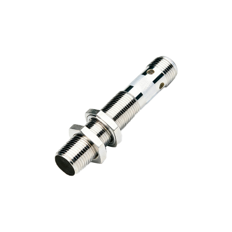
Reading these schematics requires attention to key symbols: the coil for inductive sensors, the capacitor symbol with a special notation for capacitive sensing, and the diode/transistor symbols with light arrows for photoelectric components. Voltage regulators (78xx series or low-dropout types) are standard for providing stable internal power. Engineers must also identify the output configuration symbols—sourcing (PNP) or sinking (NPN)—and the wiring for 2-wire, 3-wire, or 4-wire sensors directly from the diagram.
In practice, a thorough analysis of the proximity sensor schematic allows for effective interfacing with control systems, proper selection of load resistors, and implementation of necessary noise suppression techniques like shielded cabling and RC snubbers. It also empowers the engineer to diagnose failures, whether in the oscillator stage, the output transistor, or the power supply section. Mastering these diagrams is not just about reading symbols; it's about understanding the translation of a physical phenomenon into a reliable electrical signal, which is the essence of precision industrial sensing.