In the realm of industrial automation and control systems, proximity switch sensors stand as fundamental components, enabling non-contact detection of objects with high precision and reliability. Their manufacturing process is a sophisticated blend of material science, electronic engineering, and stringent quality control, tailored to meet the rigorous demands of diverse industrial environments. This article delves into the core aspects of proximity sensor production, from design principles to final testing.
The journey begins with the sensor's core technology selection. Manufacturers primarily focus on three types: inductive, capacitive, and photoelectric. Inductive sensors, detecting metallic objects, are the most prevalent in heavy machinery. Their production starts with the fabrication of a ferrite core and coil assembly. The coil is wound with precision to achieve the desired sensing range and frequency. This assembly is then encapsulated in a housing, typically made of nickel-plated brass or stainless steel (e.g., 303, 304, 316 grades), chosen for its mechanical strength, corrosion resistance, and shielding properties. The encapsulation process must ensure complete protection from environmental contaminants like dust, coolants, and metal shavings, often achieved through potting with epoxy resins or laser welding for hermetic seals.
For capacitive sensors, designed to detect both metallic and non-metallic materials, the manufacturing emphasizes the sensing electrode's design and the stability of the oscillator circuit. The electrode surface finish and the dielectric properties of the front face material are critical. The housing here might incorporate materials like PTFE or specific plastics to influence the field pattern. Photoelectric sensor production, conversely, centers on the precise alignment of the emitter (usually an LED or laser diode) and the photodetector (phototransistor, photodiode). This requires clean-room assembly techniques to prevent particulate contamination on optical surfaces, which could scatter light and cause false triggers.
The electronic circuitry is the brain of the sensor. Surface-Mount Technology (SMT) lines populate printed circuit boards (PCBs) with microcontrollers, oscillators, signal amplifiers, and output switching components (like MOSFETs or relays). For inductive and capacitive types, the oscillator circuit is tuned to a specific frequency. Any disturbance in this field (caused by a target object) is detected, amplified, and converted into a clean switching signal. Robust surge protection circuits, conforming to standards like IEC 60947-5-2, are integrated to safeguard against voltage spikes and electromagnetic interference (EMI), a non-negotiable requirement for sensors operating near large motors or welders.
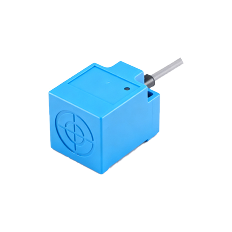
Output configuration is another key manufacturing step. Sensors are built with various output types: NPN (sinking), PNP (sourcing), analog (4-20mA, 0-10V), or IO-Link for digital communication. The assembly line configures and tests each variant accordingly. The wiring and connection method—whether pre-wired cable, quick-disconnect (M8, M12 connectors), or terminal block—is also integrated at this stage. The use of gold-plated contacts in connectors is common to ensure low resistance and long-term reliability.
Quality assurance is embedded throughout the manufacturing cycle. Incoming materials undergo inspection for dimensional and metallurgical specifications. In-process testing includes verifying coil inductance, circuit functionality, and housing integrity. The final product is subjected to a battery of tests that simulate real-world conditions. This includes:
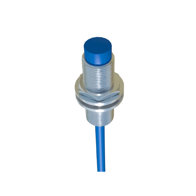
Sensing Range Tests: Using certified test targets to verify the declared switching distance (Sn) under specified conditions.
Environmental Tests: Cycling sensors through high and low temperatures, humidity chambers, and salt spray tests to validate IP (Ingress Protection) ratings (e.g., IP67, IP69K).
Electrical Endurance Tests: Subjecting the output switch to millions of cycles under load to ensure contact reliability.
EMI/RFI Immunity Tests: Ensuring the sensor operates correctly in electrically noisy environments.
Modern manufacturing facilities employ automated optical inspection (AOI) for PCBs and automated test equipment (ATE) for final functional verification, ensuring consistency and traceability. Each sensor is often laser-marked with its model number, serial number, and electrical specifications.
The trend in proximity sensor manufacturing is towards miniaturization, increased intelligence, and enhanced connectivity. The integration of ASICs (Application-Specific Integrated Circuits) allows for smaller footprints and advanced features like temperature compensation and diagnostics. The rise of IO-Link transforms standard sensors into smart devices, capable of reporting parameters like operating hours, temperature, or signal strength to higher-level control systems. This shift necessitates manufacturing processes that can handle the assembly of more complex mixed-signal circuits and firmware programming.
In conclusion, the production of proximity switch sensors is a highly engineered process where precision, durability, and reliability are paramount. From the selection of rugged housing materials to the calibration of sensitive electronic circuits and exhaustive performance validation, each step is designed to ensure that the final product performs flawlessly in demanding industrial applications,