The production of photoelectric proximity sensors represents a sophisticated intersection of optoelectronics, precision engineering, and industrial automation. These devices, essential for non-contact object detection in countless applications from packaging machinery to automotive assembly lines, demand a manufacturing process characterized by meticulous attention to detail and stringent quality control. The journey from raw materials to a reliable, market-ready sensor involves several critical phases, each underpinned by advanced technology and deep engineering expertise.
The core manufacturing process begins with the selection and preparation of key components: the light emitter, the photodetector, and the signal processing circuitry. Typically, the emitter is a light-emitting diode (LED) or, for longer-range applications, a laser diode. The photodetector is usually a phototransistor or photodiode. These semiconductor components are sourced from specialized suppliers and undergo rigorous incoming inspection, including spectral response testing for the detector and output intensity verification for the emitter. The heart of the sensor is its housing, often molded from high-grade engineering plastics like PBT or polycarbonate, designed to provide precise optical alignment, environmental sealing (commonly IP67 or higher), and mechanical robustness.
Assembly is a highly automated and controlled procedure. In a clean-room environment to prevent optical contamination, the emitter and detector are precisely positioned within their respective chambers in the housing. This alignment is paramount; even micron-level deviations can drastically affect the sensor's sensing range and accuracy. Robotic placement systems are calibrated using vision systems to ensure perfect coaxial or opposed alignment, depending on whether the sensor is designed for diffuse, retro-reflective, or through-beam operation. Following placement, the components are potted with a transparent epoxy resin. This step serves a dual purpose: it permanently fixes the optical elements and provides a protective barrier against moisture, dust, and vibration.
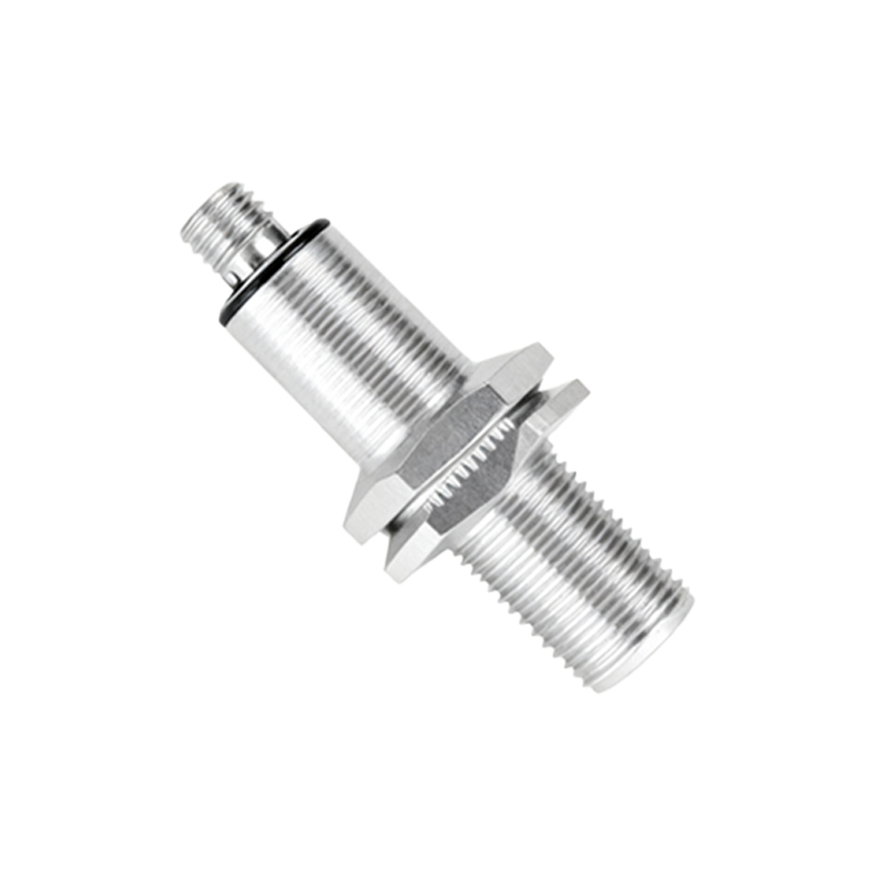
The next stage involves integrating the electronic control unit. A custom-designed ASIC (Application-Specific Integrated Circuit) or microcontroller is mounted on a PCB alongside supporting components for signal amplification, modulation, and output switching. Modern sensors employ modulated LED light (often in the infrared spectrum to avoid ambient light interference) and synchronous detection circuits. This technology allows the sensor to distinguish its own emitted light from ambient background light, ensuring stable operation in variable lighting conditions. The PCB is then connected to the optical assembly and housed within the main body. Connections for power supply (typically 10-30V DC) and output signals (PNP/NPN transistor, analog, or IO-Link) are securely terminated.
Calibration and testing form the most critical quality gate. Each sensor undergoes a battery of automated tests. Key parameters verified include: sensing distance (ensuring it meets the specified nominal range), hysteresis (the difference between the switch-on and switch-off points), response time, and temperature drift. Testing is performed using calibrated reference targets under controlled environmental conditions. Advanced test benches simulate real-world scenarios, such as detecting objects of different colors, materials, and surface finishes. For background suppression sensors, the precise cutoff distance is calibrated with extreme accuracy. Every unit is also subjected to environmental stress tests, including thermal cycling and vibration tests, to validate its durability and long-term reliability.
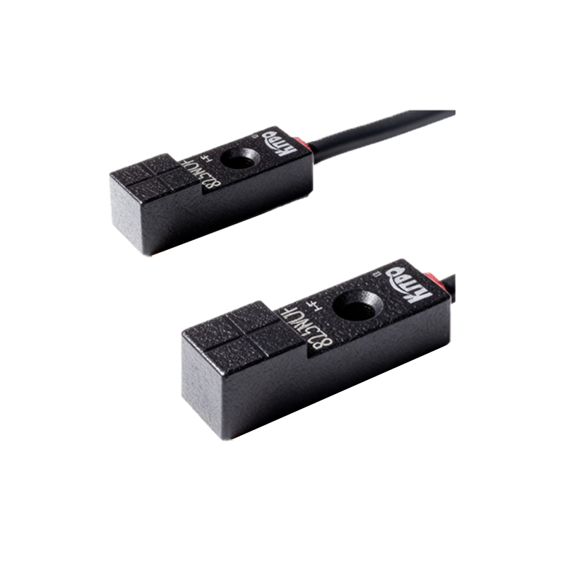
Finally, the sensors are labeled with their technical specifications, marked with laser engraving for permanence, and packaged according to customer or industry standards. The entire manufacturing line is governed by quality management systems like ISO 9001, with traceability maintained for every component. The evolution towards Industry 4.0 has further integrated smart manufacturing principles, with data from every production step collected and analyzed to enable predictive maintenance of equipment and continuous process optimization. The result is a highly reliable, maintenance-free component that serves as the essential "eyes" of modern automated systems, enabling precise, rapid, and non-contact detection critical for efficiency, safety, and quality in industrial operations.