In the realm of consumer electronics, Apple's integration of infrared (IR) laser sensors represents a sophisticated convergence of photonics, microelectronics, and advanced software algorithms. As an electrical engineer specializing in sensor systems, a deep dive into this technology reveals not just a component, but a pivotal subsystem enabling a new dimension of user interaction and device capability. This article explores the engineering principles, implementation, and broader industry implications of Apple's IR laser sensor technology.
At its core, the technology deployed in devices like the iPhone's Face ID system and the LiDAR Scanner is a form of structured light or time-of-flight (ToF) sensing. The fundamental principle involves emitting a pattern of invisible, eye-safe infrared laser dots onto a subject or scene. A dedicated IR sensor or an array of sensors then captures the distortion of this pattern as it reflects back. By analyzing this deformation with a dedicated processor like the Neural Engine, the system constructs a precise depth map or a detailed 3D model of the face. This process, occurring in milliseconds, exemplifies high-speed optoelectronic signal processing.
From an electrical engineering standpoint, the subsystem comprises several critical modules. First, the vertical-cavity surface-emitting laser (VCSEL) array. Apple's custom-designed VCSELs are marvels of semiconductor fabrication, offering high efficiency, low power consumption, and the ability to be packaged into dense arrays. They emit the coherent IR light essential for the projection. Second, the IR image sensor, typically a specialized CMOS sensor filtered to be sensitive only to the specific IR wavelength emitted by the VCSELs (often around 940nm). This sensor must have high sensitivity and low noise to function reliably in varying ambient light conditions. The third key element is the computational silicon—the Application Processor and Neural Engine. They run complex algorithms for dot pattern recognition, 3D reconstruction, and secure authentication, all within stringent power and thermal budgets.
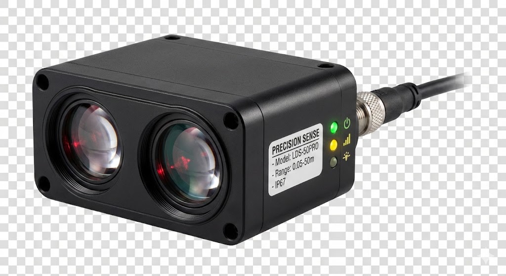
The choice of infrared spectrum, specifically near-infrared (NIR), is deliberate. NIR light is invisible to humans, ensuring user comfort and unobtrusive operation. It also generally experiences less interference from ambient visible light compared to using visible spectrum lasers, although sunlight with IR components remains a design challenge mitigated through optical filtering and adaptive power algorithms. The system's robustness is further enhanced by flood illuminators and proximity sensors that work in concert with the laser projector, ensuring functionality from complete darkness to bright sunlight.
The applications extend far beyond face authentication. The integration of a LiDAR (Light Detection and Ranging) scanner, which uses direct ToF principles with laser pulses, marks a significant evolution. Here, the system measures the time for a laser pulse to return, calculating distance with extreme accuracy. This enables transformative features in photography, such as instant autofocus in low light and enhanced portrait mode effects through superior depth mapping. In augmented reality (AR), it allows for rapid plane detection and realistic object occlusion, creating a more immersive and stable AR experience. For developers and industries, this sensor opens doors in fields like 3D scanning, interior design, assisted accessibility features, and even preliminary measurements in construction or logistics.
However, engineering such a system presents notable challenges. Power management is paramount; driving laser arrays and processing high-frame-rate depth data is computationally intensive. Apple addresses this through highly integrated system-on-a-chip (SoC) design and power-optimized coprocessors. Thermal dissipation in compact form factors is another critical concern, managed via advanced materials and dynamic performance throttling. Furthermore, ensuring data security and privacy is engineered at the hardware level, with the depth map processed in a secure enclave and never stored in raw form on the device or cloud.
Looking forward, the trajectory for IR laser sensors in Apple's ecosystem points towards greater miniaturization, enhanced accuracy, and lower power consumption. We may see their integration into a wider range of devices, from glasses to home automation products. The fusion of these sensors with on-device machine learning will unlock more contextual and predictive functionalities. From an industry perspective, Apple's large-scale adoption drives supply chain innovation in VCSEL and sensor manufacturing, pushing the entire field of consumer optoelectronics forward.
In conclusion, Apple's infrared laser sensor is not merely a "feature" but a foundational technology platform. It exemplifies how deep hardware-software co-design, leveraging advancements in semiconductor lasers, imaging sensors, and computational silicon, can create seamless and secure user experiences. For engineers, it serves as a compelling case study in integrating complex photonic systems into mass-produced consumer devices, balancing performance, reliability, and elegance.