Micro proximity sensors represent a critical component in modern automation, industrial control, and smart device applications. As a senior electrical engineer specializing in sensor technology, I will delve into the intricate manufacturing process, key design considerations, and industry best practices for producing high-performance micro proximity sensors.
The manufacturing journey begins with substrate selection, typically using materials like FR-4, ceramic, or specialized polymers for flexible sensors. Photolithography plays a pivotal role in patterning the sensing coils and oscillator circuits on the substrate. For inductive-type micro proximity sensors, a copper coil is precisely etched, with coil geometry—such as diameter, number of turns, and trace width—directly influencing sensitivity and detection range. Capacitive variants require precise deposition of electrode layers, often using sputtering or electroplating techniques to ensure uniform thickness and minimal parasitic capacitance.
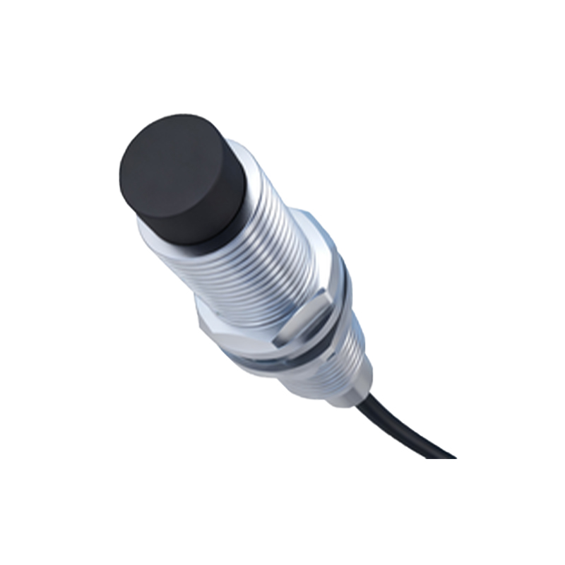
Integrated Circuit (IC) assembly follows, where the oscillator, amplifier, and signal conditioning circuitry are mounted. Advanced manufacturing employs surface-mount technology (SMT) for miniaturization, utilizing pick-and-place machines for accurate component positioning. Reflow soldering ensures reliable electrical connections while maintaining thermal stability for sensitive components. For high-frequency operation (common in sensors detecting non-ferrous metals), careful PCB layout is mandatory to mitigate electromagnetic interference (EMI). Ground planes and shielding layers are incorporated to enhance signal integrity.
Encapsulation is a crucial step, as it protects the sensor from environmental hazards like moisture, dust, and chemical exposure. Epoxy resins or silicone-based compounds are injected into molds, forming a hermetic seal around the sensing face. The material must have a low dielectric constant to avoid interfering with the sensor's electromagnetic field. For harsh industrial environments, manufacturers may use IP67 or IP69K-rated enclosures made of stainless steel or PBT plastic.
Calibration and testing form the final phase. Each sensor undergoes rigorous performance validation, including detection distance tests using standardized targets (e.g., iron, aluminum, or copper plates). Key parameters like hysteresis, repeatability, and temperature drift are measured. Automated test systems apply varying supply voltages (typically 5-24V DC) and load conditions to ensure compliance with industry standards such as IEC 60947-5-2. Sensors are also subjected to environmental stress tests, including thermal cycling and vibration resistance checks, to guarantee longevity in field applications.
From a design perspective, engineers must balance size constraints with performance. Reducing sensor size often compromises detection range, necessitating trade-offs. Recent advancements include the integration of ASICs (Application-Specific Integrated Circuits) for smarter output options (e.g., IO-Link or analog outputs) and self-diagnostic features. Energy efficiency is another focus, with low-power designs enabling battery-operated IoT applications.
In summary, manufacturing micro proximity sensors demands precision engineering, from material science to automated assembly. As industries embrace Industry 4.0, these sensors will continue evolving, with trends pointing toward higher integration, wireless capabilities, and enhanced robustness. For engineers, staying updated on semiconductor innovations and encapsulation technologies is key to driving future developments.