In the complex landscape of industrial automation, proximity sensors are indispensable components, acting as the silent sentinels that detect the presence or absence of objects without physical contact. Among these, the anti-interference proximity sensor stands out as a critical solution for environments plagued by electrical noise, electromagnetic interference (EMI), and other disruptive factors. This article delves into the schematic diagram of such a sensor, dissecting its core principles and the design strategies that confer its robust immunity to interference.
At its heart, a typical inductive proximity sensor—the most common type for metallic object detection—comprises several key stages, as revealed in its schematic. The journey begins with an LC Oscillator Circuit. This circuit, centered around a coil (L) and a capacitor (C), generates a high-frequency electromagnetic field at the sensor's active face. When a metallic target enters this field, eddy currents are induced in the target, causing a measurable change in the oscillator's amplitude or frequency. This is the fundamental detection mechanism.
However, in a standard design, this sensitive oscillatory signal is highly vulnerable. This is where the "anti-interference" architecture takes center stage. Examining the schematic, one will notice several dedicated blocks beyond the core oscillator:
1. Signal Conditioning and Filtering: The raw signal from the oscillator is weak and noisy. It is first passed through a high-gain amplifier stage. Crucially, this stage is often followed by active band-pass filters. These filters are tuned precisely to the oscillator's frequency, effectively attenuating any signals outside this narrow band. Common-mode interference and harmonics from power lines or variable-frequency drives (VFDs) are thus significantly rejected at this early stage.
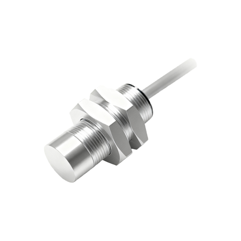
2. Demodulation and Threshold Detection: The amplified and filtered AC signal is then demodulated, converting it into a DC voltage level proportional to the oscillation amplitude. This DC signal is fed into a comparator circuit with a precisely set hysteresis threshold. The hysteresis is vital; it prevents rapid, erratic switching of the output when the target is at the borderline detection distance, which could be triggered by minor signal fluctuations due to interference. The comparator provides a clean, digital signal (high/low) indicating target presence.
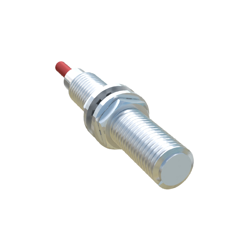
3. Shielding and Grounding Strategies (Implied in Layout): While a schematic symbol might simply show a coil, the physical implementation is key. The sensing coil is invariably housed within a ferrite core and surrounded by a robust metallic shield (often copper or aluminum). This shield, connected to a clean ground point on the PCB, acts as a Faraday cage, diverting external electric fields away from the sensitive coil. The schematic's ground symbols are not trivial; a star-point grounding scheme is typically employed to avoid ground loops, which are prime conduits for noise.
4. Output Stage Isolation: The final output stage, whether it's a transistor (PNP/NPN), solid-state relay, or analog amplifier, is a potential entry point for interference. In high-performance anti-interference sensors, opto-isolators or dedicated isolation ICs are integrated into the output path. In the schematic, this appears as a separate component that electrically isolates the sensitive sensing circuitry from the noisy load side (e.g., PLC inputs, relays, motors). This prevents back-emf, inductive kickback, and ground potential differences from corrupting the sensor's internal logic.
5. Power Supply Regulation and Filtering: A dedicated section of the schematic is devoted to power management. A voltage regulator provides a stable, low-ripple DC supply for the analog and digital circuits. Crucially, multiple stages of filtering are used: bulk capacitors for low-frequency noise, ceramic decoupling capacitors for high-frequency noise at each IC's power pin, and often a ferrite bead or inductor in series with the power line to form a low-pass filter. This ensures the "cleanliness" of the internal power rails, which is foundational for interference immunity.
Furthermore, modern digital or microcontroller-based proximity sensors incorporate advanced techniques like synchronous detection or digital signal processing (DSP). In these schematics, an analog-to-digital converter (ADC) digitizes the conditioned signal. The microcontroller can then run algorithms to perform Fourier analysis, continuously monitoring the signal's power at the operating frequency while ignoring other frequencies, or implementing adaptive filtering. This software-defined approach offers superior flexibility and noise rejection.
In conclusion, the schematic of an anti-interference proximity sensor is a blueprint for resilience. It is not merely a detection circuit but a carefully orchestrated system of amplification, selective filtering, intelligent thresholding, physical shielding, and electrical isolation. Each component, from the smallest bypass capacitor to the opto-isolator, plays a deliberate role in ensuring that the decisive "detect" or "no-detect" signal is derived solely from the presence of a target, and not from