Proximity sensors are critical components in modern automation and industrial systems, enabling non-contact detection of objects with high precision and reliability. The manufacturing process of these sensors involves a series of sophisticated steps that ensure optimal performance and durability. This article provides an in-depth look at the standard production workflow for inductive and capacitive proximity sensors, which are widely used across various industries.
The manufacturing journey begins with the design and prototyping phase. Engineers develop detailed schematics and specifications based on the sensor's intended application, such as detection range, output type (e.g., NPN, PNP, or analog), and environmental resistance. Advanced CAD software is used to create 3D models, followed by the production of prototypes for testing. These prototypes undergo rigorous evaluations to validate electrical characteristics, response time, and resistance to factors like temperature fluctuations, humidity, and mechanical stress.
Once the design is finalized, the production of printed circuit boards (PCBs) commences. The PCB serves as the core of the sensor, housing components like oscillators, amplifiers, and output circuits. The board is fabricated using automated etching and drilling machines, with copper traces carefully laid out to minimize interference. Surface-mount technology (SMT) is typically employed for component assembly, where pick-and-place machines accurately position microchips, resistors, and capacitors onto the PCB. This stage is followed by reflow soldering, which securely attaches the components while maintaining electrical integrity.
After PCB assembly, the sensing coil or electrode is integrated. For inductive sensors, a copper coil is wound around a ferrite core and encapsulated in epoxy to protect against vibrations and moisture. Capacitive sensors, on the other hand, feature conductive plates or films that form the sensing element. This component is then connected to the PCB, ensuring precise alignment to achieve the desired sensing field. The entire assembly is tested for electrical continuity and signal stability using automated test equipment (ATE).
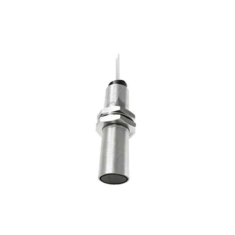
The next step involves housing and encapsulation. The sensor assembly is placed into a durable housing, usually made of materials like nickel-plated brass, stainless steel, or engineering plastics such as PBT or PPS. These materials are chosen for their robustness, corrosion resistance, and ability to withstand harsh industrial environments. The housing is designed to provide IP67 or higher ingress protection, safeguarding the internal electronics from dust, water, and chemicals. Potting compounds, often silicone-based, are injected to fill any gaps, offering additional mechanical support and thermal management.
Following encapsulation, the sensors enter the calibration and final testing phase. Each unit is subjected to functional tests to verify key parameters, including switching distance, hysteresis, and output signal accuracy. Calibration equipment adjusts the sensor's sensitivity to meet specified tolerances, ensuring consistency across batches. Environmental stress tests, such as temperature cycling and vibration simulations, are conducted to confirm reliability under real-world conditions. Quality control checks also involve visual inspections for defects in housing or labeling.
Finally, the sensors are labeled with model numbers, certifications (e.g., CE, UL), and electrical ratings. They are packaged in anti-static materials to prevent damage during shipping. The entire manufacturing process adheres to industry standards like ISO 9001, emphasizing traceability and continuous improvement. By integrating automation with stringent quality assurance, manufacturers deliver proximity sensors that enhance efficiency in applications ranging from conveyor systems to robotic arms, contributing to smarter and safer industrial operations.