The genesis of camera-based laser sensors, often referred to as laser displacement sensors or profile sensors, is a compelling narrative of converging technological disciplines. Their development cannot be attributed to a single eureka moment but rather to a sustained evolution driven by the escalating demands of precision manufacturing, quality control, and robotics. The foundational pillars for this technology were laid separately in the realms of optics, laser physics, and electronic imaging.
The first critical component, the laser, emerged from theoretical work in the mid-20th century. The term itself, an acronym for Light Amplification by Stimulated Emission of Radiation, was coined in 1957. The practical realization of the first working laser by Theodore H. Maiman in 1960, using a ruby crystal, marked a pivotal point. Early lasers were bulky and unstable, but their coherent, monochromatic light—a perfectly aligned beam of a single wavelength—presented an ideal structured light source for measurement. Engineers quickly recognized that a laser beam could act as an exceptionally straight and bright "optical ruler."
Simultaneously, imaging technology was undergoing its own revolution. The development of the Charge-Coupled Device (CCD) by Willard S. Boyle and George E. Smith at Bell Labs in 1969 provided the essential electronic eye. For the first time, light could be converted into digital signals with high fidelity using a solid-state sensor, a far cry from the analog and film-based systems of the past. The complementary metal-oxide-semiconductor (CMOS) sensor, developed later, offered further advantages in speed, cost, and integration, eventually becoming dominant.
The conceptual fusion of these two technologies—projecting a laser line or spot onto a target and observing its deformation with a camera—formed the core principle of triangulation. This geometric method, ancient in concept, found a powerful new expression. A laser diode projects a focused spot or a thin line onto the target object's surface. A lens in the sensor head images this illuminated pattern onto a CCD or CMOS array. The precise position of the laser spot or the contour of the line on the sensor pixel array shifts proportionally to the target's distance or profile. Sophisticated onboard processors then calculate height, depth, or presence with micron-level accuracy by analyzing this pixel displacement.
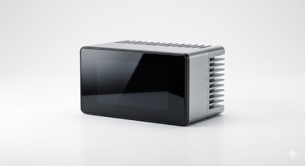
The initial industrial drivers for this integration were the automotive and electronics sectors in the 1980s and 1990s. As manufacturing tolerances tightened and production speeds increased, traditional contact probes and simple photoelectric sensors became inadequate. There was a pressing need for non-contact, high-speed, and high-resolution inspection. Early applications included checking the coplanarity of semiconductor leads, measuring the gap and flush of automotive body panels, and verifying the dimensions of precision-machined parts. These sensors provided a solution that was immune to mechanical wear and could capture full profiles instantly, not just single points.
The evolution was further accelerated by advancements in computing power and algorithm development. Early sensors relied on relatively simple centroid calculations to find the peak of a laser spot. The introduction of the laser line enabled the capture of an entire 2D cross-section in a single snapshot. Advanced sub-pixel interpolation algorithms were developed to extract resolution finer than the physical size of a camera pixel. The processing of these dense point clouds, generating accurate 3D profiles, became feasible with faster microprocessors and dedicated digital signal processors (DSPs).
Another significant milestone was the miniaturization and ruggedization of the components. Industrial environments are harsh, subjecting equipment to vibration, temperature fluctuations, and ambient light interference. Engineers developed robust housings, integrated temperature compensation circuits, and employed optical filters to isolate the laser's specific wavelength from background illumination. This made camera-based laser sensors viable for direct integration into machine tools, assembly robots, and conveyor lines.
Today, the technology has matured into a cornerstone of Industry 4.0 and smart factories. Modern laser profile sensors combine high-speed cameras with powerful class 2M or class 2 lasers, offering scan rates in the kilohertz range. They perform complex tasks like robotic bin picking, real-time weld seam tracking, online inspection of web materials, and detailed 3D contouring. The origins of this technology—from the theoretical laser and the invention of the CCD to the industrial need for non-contact metrology—demonstrate a classic case of synergistic innovation. The camera-based laser sensor stands as a testament to how converging paths in physics, electronics, and software engineering can create an instrument that fundamentally enhances our ability to measure and control the physical world with unprecedented precision.